How to Read From Slave Spi Pic32
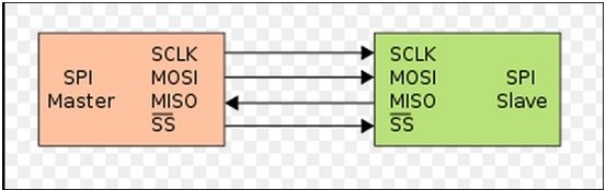
SPI stands for Serial Peripheral Interface. Like UART and I2C, Information technology is used to transfer data simply and rapidly from one device to another. About importantly, information technology has a faster data transfer rate than UART and I2C. Nosotros can utilise it to transmit and receive eight-scrap data synchronous at the same fourth dimension. Therefore, it supports full-duplex communication. SPI protocol consists of iv lines such as SDO, SDI, SCK, and CS.
It is the popular embedded serial advice that is widely supported by many chip industry. Information technology is considered as 1 of the fastest serial data transfer interfaces for the embedded organization. Most of the fourth dimension, it is used to communicate data to and from the micro-microcontroller.
SPI Communication Introduction
SPI is a synchronous protocol based on the master-slave communication type. The master device (usually a microcontroller ) controls slave devices. Because the slave device takes instructions from the master device. It allows manual of data from a master device to one or more slave devices and from slave devices to master devices over short distances at high speeds (MHz). Information technology consists of 4 fours but three-wire advice is also possible.
- MOSI/SDO: This line used to ship data to a slave. It can be read as master-out salve-in
- MOSI /SDI: MOSI wire used to receive data from a slave. It is an input line for the principal and output line for a slave.
- SCLK: Clock signal wire
- CS/SS: In case of a single master and multiple slave configuration, this wire used to select to which slave, chief device wants to send data.
SPI bus interface connectedness is incorporated into many devices like ADC, DAC, and EEPROM. If you want to explore farther on SPI communication protocol, read this complete guide:
- In-Depth Guide on SPI communication Protocol
SPI Communication Module Motion-picture show Microcontrollers
SPI is implemented in the PIC microcontrollers by a hardware module called the Synchronous Serial Port or the Chief Synchronous Serial Port. This module is built into many PIC microcontrollers. This module likewise supports II2C advice that is a ii-wire communication. Information technology supports SPI serial communication betwixt ii or more devices at a high speed and is reasonably easy to implement.
Unlike I2C, we do non utilise slave address in serial peripheral interface communication. But nosotros use a chip select pin to select a slave. In the instance of multiple slaves, we need a chip select wire for every slave device.
Moving-picture show SPI communication module transmits/receives 8-bit data synchronously simultaneously. That ways it supports total-duplex communication way.
SPI Communication Bus Pins
SPI was originally started by Motorola Corp, simply now this standard is adopted past many semi-conductor fleck companies. Information technology consists of a total of 4 pins:
- SDO: Serial information output from master and Input to slave [MOSI]
- SDI: Serial data input to chief and output from slave [MISO]
- SCLK: Serial clock output from master [SCK] Input to slave [SCK]
- CE: Chip Enable or SS (Slave Select)
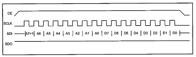
Only ii pins SDI (Data in) and SDO (Information out) are for data transfer. This reduction of information pins reduces the packet size and power consumption. SPI autobus has the SCLK (serial clock) pin to synchronize the data transfer between ii chips. Information technology is generated by the primary device and controls when data is sent and when it is read. The terminal pin of SPI bus is CE (Chip Enable) which is used to initiate or end the data transfer. When the CE signal goes low at a slave device, only that slave is accessed by SPI and volition listen for SPI clock and information signals. These four pins make the SPI a 4-wire interface. In the iii-wire interface, we have SCLK, CE and only one single pivot for data transfer.
SPI Communication Data Transfer
In connecting a device with an SPI bus to a microcontroller, nosotros use the MCU as a master device and the SPI device acts equally a slave. The clock indicate is provided by the master to provide synchronization. MCU generates the SCLK which is fed to the SCLK pin of the SPI device. The SPI protocol uses SCLK to synchronize the transfer of one bit at a time and the MSB (Most significant scrap) goes in first.
During transfer:
- CE must be high, CE=1.
- Address and data are transferred between MCU and slave in a grouping of 8 bits.
- The address byte is immediately followed by a Data byte.
- For Write: A7 flake of accost byte is always 1
- For reading: A7 bit of accost byte is always 0
SPI Information Transfer Modes
There are two modes of functioning for SPI devices.
- Single byte write
- Multiple bytes write
Single-Byte Write of SPI communication:
The post-obit are the steps to send data in a single-byte mode for SPI devices.
- Make CE=1 to begin writing.
- The viii-bit address is shifted 1 scrap at a time with each border of the clock.
- When all the 8 bits of the address are sent, the SPI device will expect to receive the data for the item address location.
- The 8bit data is shifted with one-chip time with each edge of the clock.
- Brand CE=0, which indicates the end of the write cycle.
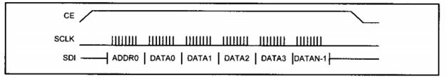
SPI Multiple Flare-up Write
This mode loads consecutive locations. We just provide the address for the starting time location, followed by the data for that location. From then on consecutive bytes are written to that consecutive memory location. SPI device internally increments the address location as long every bit CE is loftier.
Flick Microcontroller SPI Module Registers
In this department, nosotros will PIC18F452 microcontroller SPI module registers and their configuration settings. MSSP (Master synchronous serial port) module inside the Pic MCU supports the SPI protocol. Iv registers are associated with SPI of the MSSP module of PIC18F452, which are:
- SSPBUF (synchronous serial port buffer Annals)
- SSPCON1 (synchronous serial port control Register)
- SSPSTAT (synchronous serial port status Register)
- SSPSR ( Shift annals just use cannot access it)
To transfer a byte of data, it is placed in SSPBUF. This register holds the byte received. It will then transfer the contents to the SSPSR. SSPSR is the synchronous shift register for the SPI module. It shifts information in and out of the device.
SPI SSPCON1 Register
The SSPCON1 annals controls the SPI mode operation.
| bit7 | bit6 | bit5 | bit4 | bit3 | bit2 | bit1 | bit0 |
|---|---|---|---|---|---|---|---|
| WCOL | SSPOV | SSPEN | CKP | SSPM3 | SSPM2 | SSPM1 | SSPM0 |
- WCOL is a status flag that indicates if write collision error occurs.
SSPCON1bits.WCOL= 1; // i = The SSPBUF register is written while it is yet transmitting the previous word SSPCON1bits.WCOL= 0; // No fault
- SSPOV bit indicates an overflow error and this is useful in slave mode only.
- SSPEN bit (Synchronous Serial Port Enable) in the SSPCON1 annals must be fix "High" to allow the use of Pins of film MCU for SPI protocol. To enable SPI port in MPLAB XC8, we configure SSPCON1 annals like this:
SSPCON1bits.SSPEN=1 ; // Enables serial port and configures SCK, SDO, SDI, and SS every bit serial port pins SSPCON1bits.SSPEN=0 ; // Disables serial port and configures these pins every bit I/O port pins
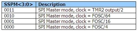
- SSPM3: SSPM0 bits are used to select SPI port manner. We tin select either main or slave style with different clock frequency options.
SPI SSPSTAT register
| bit7 | bit6 | bit5 | bit4 | bit3 | bit2 | bit1 | bit0 |
|---|---|---|---|---|---|---|---|
| SMP | CKE | D/A | P | Southward | R/W | UA | BF |
- SMP bit7: This scrap is used to sample data in chief mode and this scrap must be gear up to zero when SPI is used in slave mode.
SSPSTATbits.SMP=ane; //input data sampled at the end of information output fourth dimension SSPSTATbits.SMP=0; // input data sampled at the eye of data output time
- CKE: It selects clock edge for SPI ( positive edge or negative edge)
When CKP = 0:
SSPSTATbits.CKE = 1; // Information transmitted on rising edge of SCK SSPSTATbits.CKE = 0; // Data transmitted on falling border of SCK
When CKP = 1:
SSPSTATbits.CKE = i; //Data transmitted on the falling edge of SCK SSPSTATbits.CKE = 0; //Information transmitted on the rising edge of SCK
Buffer Total status chip:
- BF=i, receive complete, SSPBUF is full
- BF=0, receive non complete, SSPBUF is empty
Notation: Bits from 1-5 of the SSPSTAT register are reserved for I2C communication just.
SPI communication with Motion-picture show microcontroller Example
In this department, we will see example codes to utilize SPI advice with pic microcontroller in chief and slave mode. In the cease, PIC to Flick SPI communication instance will exist discussed.
Pic SPI Module Master Mode Case
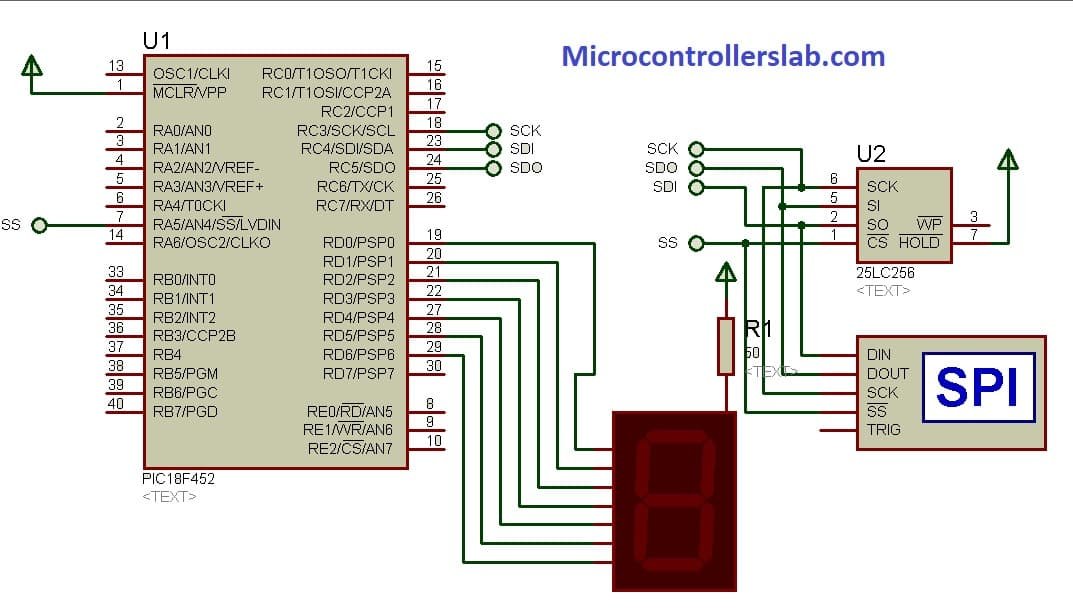
In this instance, nosotros volition learn to use the SPI module as a master. For demonstration, we use an external EEPROM (25LC256) that communicates over SPI protocol. We will write data to EEPROM with the PIC18F452 microcontroller. After that, we will read from EEPROM and display its value on seven segment display as shown in this excursion diagram.
SPI Master Mode Code PIC18F452 Microcontroller
This code uses an SPI main fashion of PIC18F452 microcontroller. Information technology will write data to external EEPROM which acts as an SPI slave device. Firstly, it will write data to EEPROM. Secondly, it will read data from the aforementioned locations and display its value on the seven segment display. Make certain to add a configuration file in this lawmaking.
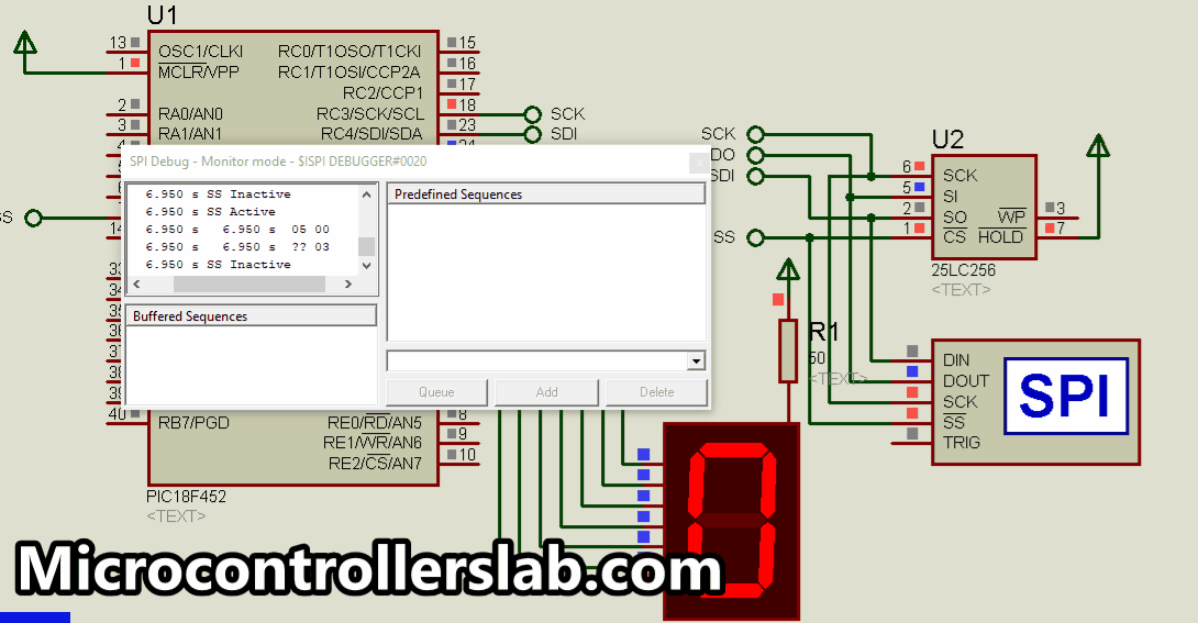
#include <ninety.h> #define SCK RC3 //Series Clock #ascertain SDI RC4 //Serial Information In #ascertain SD0 RC5 //Serial Data Out #ascertain SS RA5 //Slave Select: Not used in this application #define SCK_dir TRISC3 #define SDI_dir TRISC4 #define SDO_dir TRISC5 #define SS_dir TRISA5 #define WREN 0x06 //Write enable #define WRDI 0x04 //Write Disable #define WRITE 0x02 #define READ 0x03 #define RDSR 0x05 //Read Status Annals //----------------------Common Anode vii-Segment Codes---------------------------- char information[16] = {0xC0,0xF9,0xA4,0xB0,0x99,0x92,0x82,0xF8,0x80,0x98,0x88,0x83,0xC6,0xA1,0x86,0x8E}; /* 0, 1, 2, 3, 4, 5, 6, 7, 8, 9, A, B, C, D, E, F */ int address[16] = {0x0103,0x0B31,0x1032,0x0C23,0x6004,0xC0BF,0x10C6,0x0317,0x0AF8,0x0A19,0x102A,0x0CCB,0x1388,0x612D,0x501E,0x42AF}; /* Addresses are 16 fleck(hence int information type) broad <ie iv nibbles>(Co-ordinate to Datasheet info). NB: Called at Random */ //------------------------------------------------------------------------------ void EEPROM_write(int address,char data); char EEPROM_read(int address); char EEPROM_status(); char EEPROM_busy(); char EEPROM_wrEnable(); void delay(unsigned int nMilliseconds) { #define CYCLES_PER_MS 100 /* Number of decrement-and-test cycles. */ unsigned long nCycles = nMilliseconds * CYCLES_PER_MS; while (nCycles--); } void SPI_init() { SS_dir = 1; //Diselect fleck initially SCK_dir = 0; SDI_dir = 1; SDO_dir = 0; SS_dir = 0; //SS_dir = 0; //Disable: Because operating in chief style SSPSTAT = 0x80; //SMP = i: Sample bit. Input data sampled at end of data output fourth dimension. CKE = 0: SPI Clock Edge Select bit CLEAR SSPCON1 = 0x30; //SSPEN = 1: Enable Series Port. CKP = one: Clock Polarity Select flake: Idle state for clock is a high level } //------------------------------------------------------------------------------ void SPI_write(char data) { SSPBUF = data; while(BF == 0); } //----------------------------------------------------------------------------- char SPI_read(char dummy) { SSPBUF = dummy; //Assign to clear while(BF == 0); return SSPBUF; } #include <xc.h> void main(void) { SPI_init(); TRISD = 0; PORTD = information[0]; for( int i = 0 ; i < 16 ; i++ ) EEPROM_write(address[i],data[i]); while(ane) { for( int i = 0 ; i < xvi ; i++ ) { PORTD = EEPROM_read(accost[i]); //Pass Accost and Return value at that very address tp PORTD delay(yard); } } return; } void EEPROM_write(int address,char data) { while( EEPROM_busy() == one ); //Set up write enable latch SS = 0; SPI_write(WREN); SS = 1; //Latch-Enabled. use isWriteEn() if you want to verify //Beginning Write sequence(only occurs when/if Write latch is Enanled) SS = 0; SPI_write(WRITE); SPI_write(address>>8); SPI_write(address); SPI_write(data); SS = 1; } //------------------------------------------------------------------------------ char EEPROM_read(int address) { while( EEPROM_busy() == one ); //Wait for previous Write/Read operations to finish SS = 0; SPI_write(READ); SPI_write(address>>8); //Upper Byte SPI_write(address); //Lower Byte char data = SPI_read(0); SS = 1; return data; } //------------------------------Used every bit a flag---------------------------------- char EEPROM_status() { SS = 0; SPI_write(RDSR); //Intsruction: Read Status register of the EEPROM char condition = SPI_read(0) ; //Ship a Dummy parameter to read. Thus Any int number is valid SS = 1; return status; } //------------------------------------------------------------------------------ char EEPROM_busy() { char busy = EEPROM_status(); render (busy & 0x01); //LSB is Write-In-Process (WIP) bit. When Set, a write is in progress, when Articulate, no write is in progress } //------------------------------------------------------------------------------ char EEPROM_wrEnable() { char isWrite = EEPROM_status(); return (isWrite & 0x02); //Flake 2 is the Write Enable Latch (WEL) bit and indicates the status of the write enable latch } Simulation Effect
Film to PIC SPI Communication MPLAB XC8 Compiler
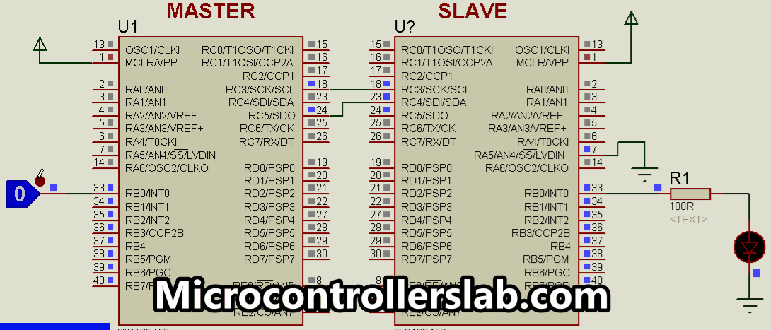
In this example, we use one pic microcontroller (PIC18F452) every bit a chief and one as a slave. The master microcontroller sends an education to the slave PIC18F452 to control an LED. Make connections according to this circuit diagram:

- Connect SCK pin of master with SCK of slave pic microcontroller
- Connect SDO pin (chief) to SDI (slave)
- Master input is a logic probe. When the user will press this probe, the master SPi device will send an instruction to the slave to control an LDE.
- Connect an LED with RB0 pin of slave motion picture microcontroller
Simulation Outcome
Moving picture SPI Master Code MPLAB XC8
Upload this code to the master-microcontroller and brand sure to add configuration file in this lawmaking. You can generate configuration bits with mplab xc8 compiler.
#include <xc.h> #include "newxc8_header.h" // generated configuration bits header file void delay(unsigned int nMilliseconds) { #define CYCLES_PER_MS 100 /* Number of decrement-and-test cycles. */ unsigned long nCycles = nMilliseconds * CYCLES_PER_MS; while (nCycles--); } void SPI_init() { // this setting selects primary mode with frequency fosc/4 SSPCON1bits.SSPM0 = 0; SSPCON1bits.SSPM1 = 0; SSPCON1bits.SSPM2 = 0; SSPCON1bits.SSPM3 = 0; // Enable SPI Port SSPCON1bits.SSPEN = i; // Configure The Clock Polarity & Phase SSPCON1bits.CKP = 0; SSPSTATbits.CKE = 0; // Slew rate control enabled for High Speed mode SSPSTATbits.SMP = 0; // Set SPI pins as digital I/O TRISC5 = 0; // SDO -> Output TRISC4 = one; // SDI -> Input TRISC3 = 0; // SCK -> Output //Uncommnent this line, if you want to send send over interrupt // SSPIE = 1; PEIE = 1; GIE = 1; } //------------------------------------------------------------------------------ void SPI_write(char data) { SSPBUF = information; while(BF == 0); } //----------------------------------------------------------------------------- void main(void) { SPI_init(); TRISB=0x00; while(1) { if(RB0) SPI_write(0x01); // if switch pressed, transport 0x01 else SPI_write(0x02); // if switch is pressed pressed, transport 0x02 } return; } PIC SPI Slave Code MPLAB XC8
#include <xc.h> #include "newxc8_header.h" char data; void __interrupt() ISR(void) { if(SSPIF) // check if interrupt occurs due to SPI module { information = SSPBUF; // copy data from receive buffer into a global variable information SSPIF = 0; // reset flag interrupt for SPI module } } void delay(unsigned int nMilliseconds) { #ascertain CYCLES_PER_MS 100 /* Number of decrement-and-exam cycles. */ unsigned long nCycles = nMilliseconds * CYCLES_PER_MS; while (nCycles--); } void SPI_init() { // Set Spi Way To Slave + SS Enabled SSPCON1bits.SSPM0 = 0; SSPCON1bits.SSPM1 = 0; SSPCON1bits.SSPM2 = 1; SSPCON1bits.SSPM3 = 0; // Enable The Synchronous Serial Port SSPCON1bits.SSPEN = 1; // Configure The Clock Polarity & Phase (SPI Way Num. 1) SSPCON1bits.CKP = 0; SSPSTATbits.CKE = 0; // Clear The SMP Flake SSPSTATbits.SMP = 0; // Configure The IO Pins For SPI Primary Mode TRISC5 = 0; // SDO -> Output TRISC4 = ane; // SDI -> Input TRISC3 = 1; // SCK -> Intput TRISA5 = 1; // SS -> Input // Enable Interrupts. Annotate Them To Disable interrupts(NOT Recommended) SSPIE = one; PEIE = 1; GIE = 1; } void primary(void) { SPI_init(); TRISB = 0x00; while(1) { if (data==0x01) { RB0=1; //if received data = 0x01, plough on LED } else if (data==0x02) { RB0=0; //if received data = 0x02, turn off LED } } return; } Movie to PIC SPI Communication Example
The main devices used in the circuit are the two 18F452 (one acts every bit a master and one as a slave) and LEDs. The 4 SPI control lines connect the two PICs together.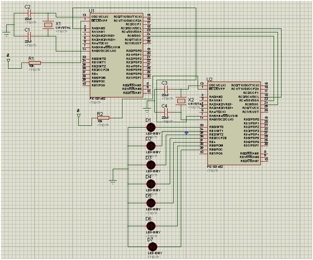
- SCLK: RC3 (master)to RC3 (slave)
- MOSI: RC5 (master) to RC4 (slave)
- MISO: RC4 (primary) to RC5 (slave)
- SS:RA0 (principal) to RA5 (slave)
7 LEDs will be used to display the data transferred to the SPI slave Moving-picture show MCU from the SPI master Pic MCU. The LEDs are connected to PORTB (RB0-RB6) of the slave Flick.
Code SPI communication with moving-picture show microcontroller
There volition be ii codes for this instance. One for the SPI master and one for SPI slave.MPLAB code is given below for both devices.The master is sending commands and slave is receiving and displaying it on the LED output port. LEDs act like a binary counter, counting downwards to zero.
SPI communication Master Code:
void primary(void){ unsigned x = 0xFF; unsigned mask = 0x80; TRISA = 0x00; TRISC = 0x00; PORTA = 0x03; OpenSPI(SPI_FOSC_16, MODE_10, SMPMID); while(1){ PORTAbits.RA0 = 0; //Slave Select putcSPI(x); PORTAbits.RA0 = 1; //Slave Select Delay10KTCYx(75); if(ten == 0) x = 0xFF; else ten--; } } SPI advice Slave Lawmaking:
void principal(void){ unsignedchar x; ADCON1 =0b00000110; //PORTA All Digital TRISA =0xFF; TRISB =0x00; PORTA =0x00; PORTB =0x00; TRISCbits.TRISC3 =1; //SCLK TRISCbits.TRISC4 =1; //MOSI OpenSPI(SLV_SSON, MODE_10, SMPMID); while(1){ while(!DataRdySPI()); 10 =getcSPI();//ReadSPI(); PORTB =(x>>1); Delay10KTCYx(5); } }
Source: https://microcontrollerslab.com/spi-communication-pic-microcontroller/
0 Response to "How to Read From Slave Spi Pic32"
Post a Comment